How Computers Work - Part 2
The Story So Far
On our intrepid quest to understand how computers actually really work, we’ve thus far covered all of the software-y bits - how a UI action can be represented in high level code, and how that high level code actually sits on top of (many layers) of lower level code until we get down to binary.
To complete the picture, in this blog post we will talk about the other half of the equation - the hardware.
Okay, Bool me over!
Before we talk about transistors and silicon though, we need to understand a little bit of the theory underpinning it.
Interestingly, the mathematics behind our modern CPU designs were developed well before the modern computer came about, invented by a man called George Bool. He (in 1847 no less), published the book “The Mathematical Analysis of Logic”, laying out what we now come to know as Boolean algebra, or Boolean logic.
Boolean algebra concerns itself with combining two states, True (1) and False (0), using 3 different basic operators (AND, OR and NOT). This differs from elementary algebra which concerns itself with combining numbers, using our familiar mathematical operators (add, subtract, multiply, divide etc).
The most basic example of Boolean algebra in action is the AND gate.
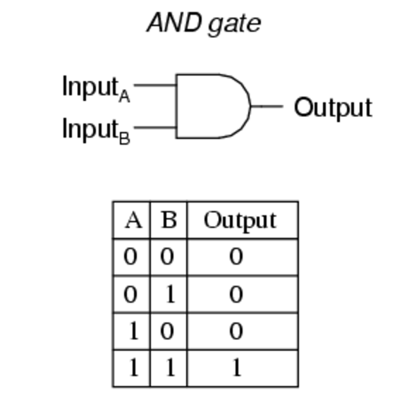
Fig 1: AND Gate
The symbol at the top is how we represent this in our diagrams, and the table shows all the possible combinations of inputs into the gate and the resultant output (e.g. the output is only true if BOTH inputs are true).
Although the mathematical framework around working with true and false values was theoretically interesting, it took until the 1930s for another man called Claude Shannon to realise its potential in concert with electronic switching circuits. For he realised that the true and false states that could be combined in Boolean algebra corresponded very well with the two different states an electronic circuit could have: some electricity flowing (true), or no electricity flowing (false).
This, as far as I am aware, is also why all of our modern electronics and computers run on binary - it is easy and reliable to represent an on (1) and off (0) state with electricity, but difficult to represent more.
Logical Progress
Remember from our previous post that what we are trying to do is to calculate the devilishly tricky sum of 1 and 1. This kind of looks like something that a logic gate could perhaps perform, doesn’t it? Maybe not the AND gate, where if we put 1 and 1 in both inputs, we get 1. But, perhaps some combination of logic gates can allow us to make this calculation.
Knowing that our logic gates can only accept a binary input (0 or 1) and provide a binary output, we need to understand what 1 + 1 is in binary. The answer is not 2, but rather 10.
BINARY 		DECIMAL
1 +		1 +
1 =		1 =
10 		2
Can we find a set of logic gates that would give us this kind of input to output mapping? Yes we can. It is a design called a “Half Adder”, and it looks like this:
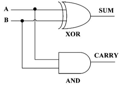
Fig 2: For some reason when I read 'Adder' in this context I think about the snake.
In this diagram, XOR means “Exclusive OR”. The output from this gate is 1 strictly if one of the inputs is 1 and the other is not. This is different from a regular OR gate where the output is 1 if either of the inputs are 1 but also if both of the inputs are 1. An XOR gate can be created by the combination of several NOT and AND gates.
We end up with two outputs from this half adder, because we need an output to represent the sum, and also one to represent the carry (remember that 1 + 1 in binary is equal to 10, where the first character (or bit) is the carry, and the second the sum). This is much like in decimal addition, where if you do 9 + 1, the result is 10 because you have to carry the 1 after you get beyond 9.
This can perhaps be more easily represented by looking at the truth table for the half adder.
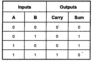
Fig 3: Half Adder Truth Table
Notice how the carry and sum combined give us the right output for the binary addition of the two inputs.
We should take stock at this point because we’ve arrived at a conceptual breakthrough! Through the mathematics of boolean algebra, we have concocted a theoretical system that can perform the addition of two 1-bit numbers.
Now, the next question we need to answer is: how do we translate this conceptual sequence of logic gates into an electronic circuit?
Enter the Transistor
In order for our theoretical logic gates to be realised in an electronic circuit, what we needed was an electronic component that could behave as a switch that could be activated electronically, and that component, when it was eventually invented, was called the transistor.
Now, to be clear: there were devices that operated like the transistor prior to the invention of the transistor, but the transistor was a key invention in enabling subsequent breakthroughs because it had no moving parts and therefore could be switched very quickly between ON and OFF states, and it was also relatively easy to miniaturise (such that we are now building transistors that are on the scale of 10’s of nanometers).
There are a few different types of transistor, and they also have another use in circuitry which is for signal amplification, but for our case, we are going to talk about using transistors (specifically MOSFETs) as switches.
![]()
Fig 4: (Left) A MOSFET which you might use in a DIY project. (Right) The circuit diagram symbol.
I’m not going to talk in detail about how a transistor works, instead, if you’re interested you can watch this explanatory video here.
For our purposes, all we need to know is that it is an electrically operated switch - if we apply a voltage at the Gate, then we close the circuit between the Source and the Drain and allow a current to flow. Conversely, if no voltage is applied at the Gate, then the circuit is broken and no current flows between the Source and the Drain.
Crucially, transistors allow us to build circuits that represent logic gates. For example, here is an AND gate:
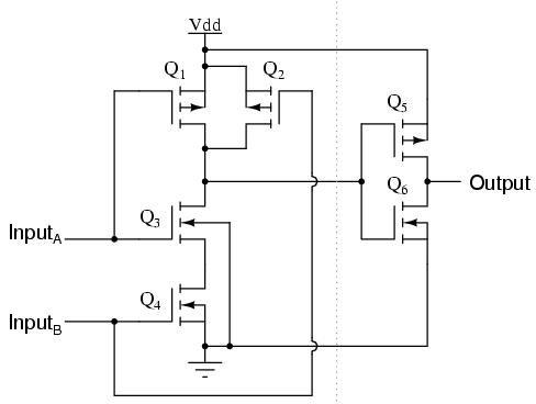
Fig 5: AND gate circuit
And, here is an XOR gate.

Fig 6: XOR gate circuit.
Now, let’s recall that our half adder circuit was actually a combination of an XOR gate to calculate the sum, and an AND gate to calculate the carry (see Fig. 2), and so we realise that if we put the above two circuits together (i.e. set both circuits’ inputs to be the same), then the outputs will be our sum (from the XOR gate circuit), and our carry (from the AND gate circuit).
Whew!
If we were to solder these circuits up and connect them to our inputs A and B, then we would have made a simple calculator that could add two 1-bit numbers together. Putting lightning into rocks and tricking them into thinking, amirite?
Scaling Up
Great as all that might be, we quickly realise that having a 1-bit calculator isn’t very useful, because the only operations we can do with it are 1 + 0 or 1 + 1. In order to deal with larger numbers we have to increase the number of bits (and so as computing advanced, we went from 8-bit to 16-bit, to 32-bit, to our now current 64-bit standard).
In order to make more than 1-bit calculations work, our “Half Adder” circuit needs to be modified into a “Full Adder” circuit. The only difference is that th eFull Adder will be able to take 3 inputs - our two bits to be added, and a carry-in value. This lets us chain a whole bunch of Full Adders together to make calculations on numbers with many bits.
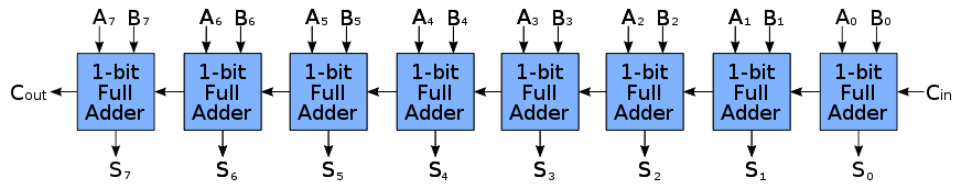
Fig 7: Eight adders chained together.
So, how does chaining a bunch of Full Adders together work? It’s simpler than you think.
Remember the process of long addition, where we started by working from the rightmost digits, calculating the sum and carry, then moving onto the tens, calculating the sum and carry taking into account any previous carry, and so on?
Well, that’s it.
Home Stretch
Okay, let’s take a breath. The super low level electronic circuit stuff is over. If you have understood everything above, I think it’ll be safe to say that you now have a fairly decent mental map of how things work from clicking something in a UI down to how electrons are shoved around inside a MOSFET.
If you haven’t, then I’m sorry for not being able to explain things in a clear enough way - please let me know in the comments and I’ll be happy to answer any follow up questions!
We just have a few pieces to fill in to complete the picture, because the ability to perform numerical calculations is only one component of a modern CPU - it is a component commonly known as the ALU (Arithmetic and Logic unit).
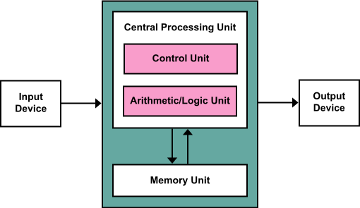
Fig 8: This model underpins pretty much all modern CPU design.
The one quirk of Von Neumann Architecture that is both good and bad is the single memory pool - this means that instructions and data are stored in a shared pool of memory. Apparently, this feature is what enables a lot of our current high level languages to exist - that the machine can process instructions that directly modify the instructions that it can run because it is in a shared memory location.
From the diagram above, we can see that the CPU is comprised not just of an ALU, but also a Control Unit - if we want to drill down into what the control unit is comprised of, it would again be a whole bunch of transistors (and other components) arranged in such as way as to implement logic gates, which are the representation of what we require the Control Unit to do - which is, namely, to accept instructions from the input device, read and write to memory as required, send computations to the ALU and receive results, and send outputs to the output device.
Remember we were talking in the previous post about instruction sets? This is why. The Control Unit has implemented these instruction sets at a hardware level (e.g. transistors on a circuit board), so that if you pass it the instruction 0010 0001 0000 0100, the circuit will perform the LDA operation from Memory Location A.
And finally, we have memory - again, these are nothing but logic gate designs translated into transistors on a circuit board (see here for an overview).
And We’re Done!
In these two blog posts, I have attempted to scratch the surface and pull together many disparate sources to, I hope, explain in a cogent way the missing pieces that I always had in my mental map of how computers worked.
It has certainly been a journey of much googling, wikipedia reading and not a little thinking, and I hope that I have been able to take you, dear reader, with me on this journey of discovery.
It goes without saying that we could pick any one of the topics briefly explained above and write entire blog posts, theses and PhDs on them, but ain’t nobody got time fo’ dat (unless you are actually doing a PhD in Digital Electronics or Computer Science, in which case, more power to you!).
As always, I welcome any comments to point out inaccuracies or questions on confusing points which I will do my level best to clarify.
Till next time!
-qz